 |
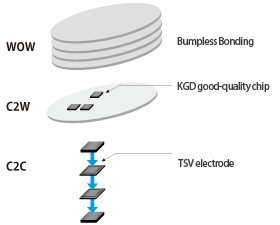
LSI has achieved high performance and low power consumption by micro-fabrication
technology. Nowadays because of the current issues such as increasing leak
current caused by the minimization of the physical size, technical limitation
of wavelengths in photolithography process, etc., another technology by
three-dimensional integration that helps to enhance the LSI performance
has come to the front. Three-dimensional integration, making shorten the
IC path and is of advantage to the enhanced performance like size reduction,
faster connection and low power consumption. Furthermore, compared to the
lamination between chips or lamination between packages, there are great
hopes towards the 3D-integration at the wafer level that it achieves higher
productivity and higher performance. |
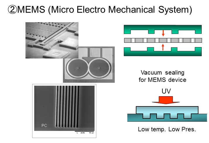
| Because MEMS device has characteristic elements with moving parts, protective packages for them are of increasing importance. Wafer Level Package (WLP) become mainstream in MEMS package, encapsulation in wafer level makes reduction of test process and drastic downsizing. In addition, surface-activated bonding has been applied due to the need for hetero wafer bonding. |
 |
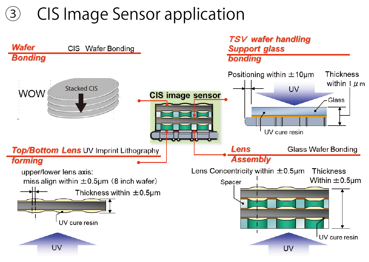
| By applying nanoimprint technology to MEMS, we have entered the commercial stage of using resin lenses. With low cost and heat resistant lenses, electrodes (TSVs) and wafer level mounting, "wafer level camera modules" are expected in the future to implement all camera module processes including image sensors and lenses. This CMOS image sensor is expected to play an active role not only in mobile phones but also in notebook computers and convenient game consoles. In addition, CMOS image sensors are attracting attention in the automobile industry. In recent years, 3D-pacaged high-speed image sensors have also been developed, and high-precision loading at the wafer level is accelerating. |
 |
| Fields where even higher definition is progressing. We bond dissimilar
materials with different thermal expansions at room temperature to achieve
high-precision bonding. |