| Bondtech develops and supplies manufacturing system for Semiconductor, MEMS (Micro Electro Mechanical Systems) devices and nanoimprint, with proprietary ultra high accurate alignment technology. Our advanced system achieved Ten Nanometer alignment with Piezo-6axis alignment system and the recognition system called "MagicVision" to precisely recognize position image by infrared-transparent . Under the guidance by Professor Tadatomo Suga of Tokyo University who has leaded the surface activated room temperature bonding technology, which is the key technology to semiconductor three-dimensional multilayer method, we developed the bonding process system at the wafer-level with surface activation technology. By this technology, it can be realized that mass-production of three-dimensional LSI, wafer or chip bonding in low vacuum or in the air. Its bonding technology helps to make MEMS hybrid devise. We select better surface activation bonding techniques most suitable to bond different semiconductor materials such as Au, Cu, Si and glass. Conventional photolithography semiconductor manufacturing has come to the limitation in the high integration and speed for the electric circuit. Bondtech's technology helps semiconductor wafer / chip bonding and three-dimensional LSI mass-production. MEMS device has structural movable parts. The bonding technology provides easier integration with electric circuit. Bondtech also has been developing nano-in-print that is nanometer pattern transcriptional equipment by photo-polymer. In the near future it is expected that existing photolithography method would be transferred to nano-in-print method in semiconductor / MEMS manufacturing technology, and three-dimensional stacking by wafer bonding technology. With our technology, customer just changes stepper to nano-in-print, and applying wafer bonding technology at the end of front-end wafer processing equipment, then gets the advance manufacturing technology without changing production method. |
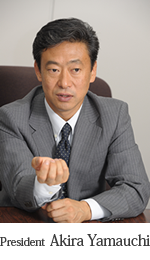 CEO Akira Yamauchi |
| I established Bondtech that a company has the unique and proprietary technology, started from a venture-incubate-room after "Creation" law authorization by Japanese government. Clear decision in offense and defense helped the company to grow in investment for the research and development with cost reduction at the same time for 20 years. Always improving the own strengths over the others, maintaining the speed as our company's lifeline, we have executed forward developing the new fields. The strength of bondtech is not an equipment supplier but a member of the research consortium which helps to determine the future of the research activities. We sometimes make a proposal by ourselves from the live information. Bondtech is the only manufacturer that can propose from chip bonder to wafer bonder including process. We can quickly and easily understand problems and provide feedback by keeping track of front end (e.g. sales and customer contact) and back end (e.g. equipment adjustment and CS) of the project. We are able to achieve commercialization in half a year, where it takes 3 years for large companies, while making early trial and error in the hypothesis testing routine by taking advantage of the speed of development. This can be achieved from the unity and concentration of members with the same aspiration, and the proof of results supported by our high technical capabilities. Based on high technology and ideas, and differentiated intellectual property, we have strength in speed and develop business that cannot be done by other companies.. |
| 会社名 | Bondtech Co., Ltd. |
| Establishment | 21, April, 2004 |
| Paid-in Capital | 47million yen |
| President | Akira Yamauchi |
| Address | Head quarters:25, miyanohigashicyo, kisshoin,Minami-ku, kyoto 601-8305
Japan TEL: +81-075-748-6180 FAX: +81-075-748-6179 |
| Description of Business | Manufacture, development and sale for Bonder and nano system for semiconductor and MEMS |
| History of development | 2004 High precision Chip Aligner “CA300” 2005 High precision vacuum wafer aligner “WA9000” 2006 Surface Activated Wafer Bonding Kit for R&D “WP-100” 2007 Plasma Surface Activated Bonding Cassette to Cassette Full Automation System, for Mass Production “WS1000” 2006-2007 NEDO 2006-2007 Grant for Venture Project “20nm Precision Alignment” 2008 Ultra High Vacuum Surface Activated Bonding System “SAB1000” 2009 Automatic Tensile Tester in Vacuum “NI1000” 2010 High precision COW for Mass Production “SCW1000” 2011 High precision UV nanoimprint S&R “SR1000” 2012 Surface activated WOW system for 12 inch (Optional; vapor assist, Si sputter) 2013 High precision COC bonder “SCA1000” 2014 Cu reductive activation bonding system “CG100” 2015 Vacuum hydrophilic bonding system for 12 inch wafer for CIS mass production“WS3000 2016 MEMS resin bonding system “WM2000” for thin wafers 2017 COW system “HB / CW3000” for hybrid bonding 2018 Multi SAB compatible wafer bonder for R&D to mass production “WFP1500” 2019 Development of accuracy inspection equipment after bonding IR wafers 2020 12"High-accuracy low strain ultra-high vacuum wafer bonder WF3000 2021 Developed real-time blade test and IR observation machine - IRC3000 2022 High accuracy WOW system for Hybrid Bonding - HBWS3000 2023 Cluster type WOW systm - WS1500 |
| ・Committee of the Japan Institute of Electronics Packaging, Kansai branch ・Auditor and Board member of Institute for Advanced Micro-system Integration (IMSI) ・Member of the 3D wafer bonding |