| Under the guidance of Professor Tadatomo Suga of the University of Tokyo,
a leading expert in the "room-temperature bonding process using surface
activation," a key technology in semiconductor 3D integration, Bondtech
has focused on developing technologies that enable low-vacuum and atmospheric
pressure bonding in the atmosphere, enabling mass production. The merit
of SAB is its ability to directly bond heterogeneous materials at room
temperature without adhesives. This will pave the way for new materials,
such as solar cells and saw filters, by directly bonding heterogeneous
materials rather than epitaxial growth, and will create groundbreaking
new fields in 3D integration. In fact, mass production has already begun,
particularly in the materials field. Furthermore, we use different surface
activation methods optimal for each bonding material. Furthermore, we have
applied a unique process to the conventional atomic beam method, lowering
the vacuum level from ultra-high vacuum to achieve the bonding of heterogeneous
materials. ①Ar etching SAB in UHV|different materials such as compound semiconductor etc. Firstly, traditional room temperature bonding method is Ar etching by FAB in an ultra-high vacuum. This method is to remove the oxide film and contaminants on the bonding surface by Ar neutral atom etching in an ultra-high vacuum, then to create dangling bond on bonding interface for the connection atoms. This method uses Ar neutral atoms, which are weaker than plasma, to etch only the surface layer, revealing a new surface and breaking the bonds between molecules and atoms to expose active surfaces that form the bonding species on the outermost surface. After performing that on both side of bonding interface, atomic level bonding is carried out by having the bonding interface contacted each other in an ultra-high vacuum. By this process, room temperature bonding of different materials is achieved, such as chemical compound semiconductors and the like which are normally hard to bond. In order to avoid recontamination of the molecules, 10-10torr ultra-high vacuum is required, and it is an obstacle to shift to mass production. Bondtech made possible to do large area uniform bonding with lower vacuum level by our unique treatment even in this ultra-high vacuum process. 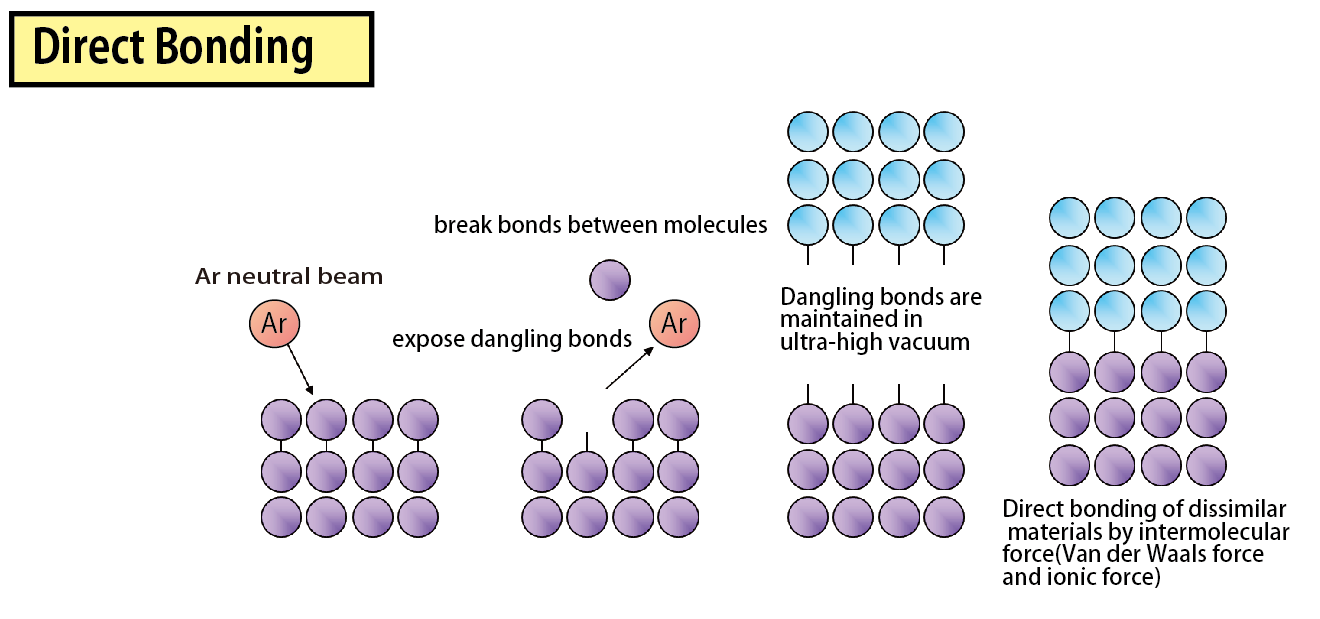 ②Oxide bonding by Si nano adhesive layer Secondly, there is a point that the ion crystalline material cannot be bonded in SAB. They are such as an oxide film or a nitride film that are wanted to bond material in the semiconductor, so this is a cause applicable to the semiconductor has been delayed. One solution for this issue is the application to the above-described hydrophilic bonding and another is a system of Si sputtering or Si-FAB as an intermediate layer between the activation treatment alternatively. Si atoms to the extent that less than 1 layer in this manner made it possible to bond in ionic crystal material by the interposition of the interface. The application can be applied to any material. 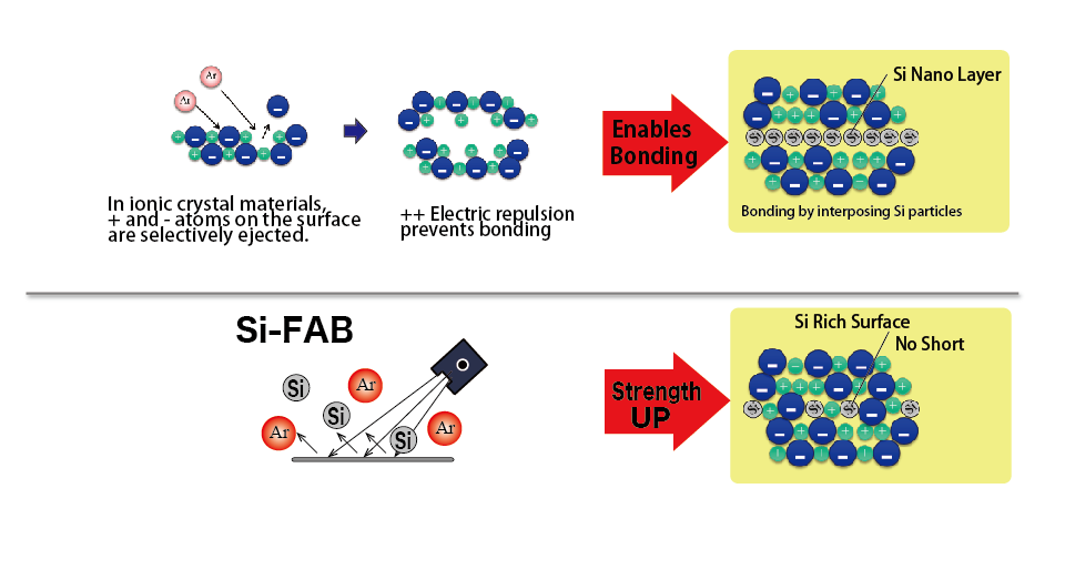 |
| For example, by activating the surface even in currently used processes,
bonding can be performed at low temperatures and in a short time, improving
alignment accuracy and throughput, and obtaining an ideal bonding interface
without an oxide film. In this way, it is also effective in improving processes
that are already in use for mass production. In the fields of 3D packaging
and MEMS, it has started as an improvement to current processes. ①Surface activated bonding of metal sealing By separating Main bonding(High Pressure) after room temperature bonding(temporary bonding) in a vacuum by FAB, we have established a process that can withstand mass production. . 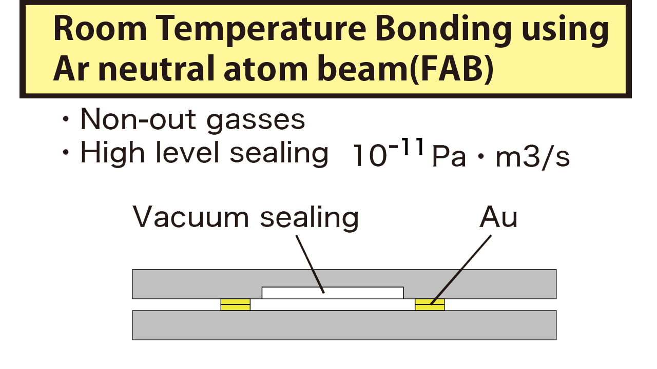 ②Anodic Bonding by SAB for MEMS Thirdly, this can be applied to conventional anodic bonding. Alkali in the glass is taken apart in high temperature of 400 degrees C. And it attracts an oxygen ion by applying the anode voltage and do covalent bond to Si. For this high temperature, it needs two hours for one wafer of bonding, including heating, cooling. Modify by SAB, It can bond at low temperature for a short time without supplying oxygen to the bonding interface by handling surface activation with the plasma in advance, and temperature at the alkali decomposition is not needed It succeed in the bonding at 200 degrees C for 15 minutes and can get throughput of 4 times. In addition, it enable the anodic bonding without getter materials because the out gas in the cavity decreases. 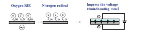 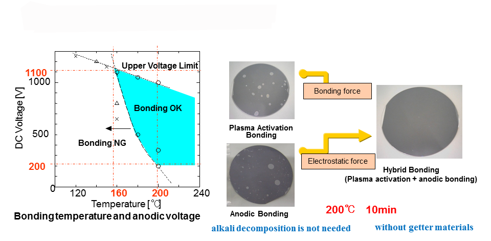 ③Hydrophilic bonding for CIS, MEMORY Third, this can be applied to conventional hydrophilic bonding in the atmosphere. In this field, it is activated with RIE plasma, but cannot produce the enough OH group. Therefore it can secure a bond strength only in the atmosphere, which water is used. Atmospheric bonds usually create some voids. Therefore, the wafer is bent and the bonding portion is extended from the center to the circumference by center push. Also, excess water molecules are microvoided during annealing. For it, modify by SAB, It can find a bond strength in vacuum by giving radical processing after RIE processing called the sequential plasma activation can increase OH groups and becomes able to improve the bond strength in the vacuum. In addition, even a method to increase the quantity of the OH group of the bonding interface by irradiating with Ar beam containing Si atoms processing. The generous since excess water molecules is removed, generation of microvoids is also suppressed. removal becomes needless without involution of the air in vacuum bonding. In addition, the bonding accuracy improves because it does not bend a wafer. . 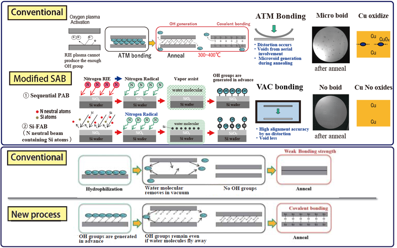 |
Equipment technology


| I introduce High Accuracy Alignment System for UHV So far, wafer is aligned in the atmosphere and clamped a wafer by a jig, and is transferred to chamber, and a spacer is taken off, and to bond in a vacuum chamber. However, there was a problem to produce a position slip when it is heated or when a spacer is pulled in vacuum chamber. However our method can bond without a position error by IR camera and recognize it just before the bonding in vacuum chamber. In addition, the function to correct a position error at the contact can keep accuracy after the bonding of +-0.2μm in the 300mm wafer. Piezo is used in UHV as the actuator and image processing is used to recognize alignment with an infrared transmission camera from the outside of the chamber. This is constructed by the software called MagicVision that even the image with bad contrast can highly recognized by the infrared transmission and the piezo actuator having the system to align of 6 axial directions. Different from X,Y,θ, 3 axis alignment such as the exposure machine, 6 axis aligning that each blast direction included becomes important not to misalign even if the pressure is applied to two surfaces.. 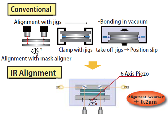 |
| ①Equipment for mass production in UHV Firstly, a disadvantage of the SAB is that a vacuum degree UHV is necessary. In the environment UHV, there was the problem that it was hard to use in the mass production equipment. It is used in R&D because it needs baking and time for a vacuum. However, by arranging the highly efficient road lock chamber to a bonding chamber, it do wafer handling in the atmosphere now and succeed in the throughput improvement of 6 minutes per wafer. ②Ar Beam Source(FAB) for Scanning Large Area up to 12'' Secondly, Even if the small sample could work in the Ar beam source, it was not able to handle the wafer level. 2 inches of wafers are limits, therefore it cannot go from the area of R&D. Then we developed Line type Ar beam source. It can be scanned to a large are. To the mass-produced equipment can apply it to 12 “ wafers. 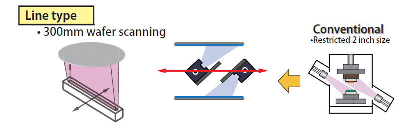 ③Special Beam Source for Si Nano-adhesion Layers Thirdly, we developed Special Beam Source for Si Nano-adhesion Layer. In this method, it can apply to any materials and application, bonding by sputtering a Si atom among the interface. In addition,. It succeeds by scanning it while changing the direction of the Ar beam source with the activated processing by the Ar beam source for a device, and irradiating a Si target. 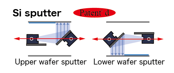 ④Si-FAB Simultaneous irradiation of Si atoms with Ar or N2 beam irradiation prevents Si from becoming a layer and creates a Si-rich interface. As a result, even when bonding with electrodes, the bonding strength is increased while maintaining insulation without shorting. Also suitable for bonding SIC in which Si depletion sites occur due to selective etching.. 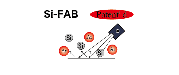 |